
D Flip-Flop Explained: Truth Table, Circuit and Timing
A D flip-flop is a one-bit memory circuit with a data input, D, and a clock input, CLK. At each active clock edge, usually the rising edge where the clock goes from 0 to 1, the output Q takes the value of D. Between edges Q holds that value whatever D does, and the second output, Q-bar, is the opposite of Q in normal operation. It is the basic storage cell of clocked digital circuits.
It is also called a D-type flip-flop, a data flip-flop or a delay flip-flop. Below the symbol there is a working one, built from NAND gates, that you can clock yourself.
The circuit below works without an account: click its inputs as often as you like. On a computer or tablet, the full lab is limited without an account: you get one of each part, and a flip-flop needs ten NAND gates. A free account gives you about 10 minutes of the full lab, and a plan removes the limits. Create a free account.
The D flip-flop symbol
The small triangle at the clock input means the flip-flop is edge-triggered: it acts at the moment the clock changes, not for as long as the clock is high. A plain triangle means the rising (positive) edge; a small circle, a bubble, in front of it means the falling (negative) edge. Flip-flop chips often add preset and clear inputs, which force Q to 1 or 0 without waiting for the clock. A D latch is drawn without the triangle, and its enable input is labelled EN or G.
Try it: a D flip-flop you can clock
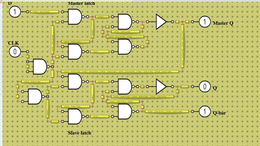
This circuit is a positive-edge D flip-flop built from NAND gates in the DCACLab lab. The lab has no flip-flop part and no clock generator, so you are the clock: click the CLK input to switch it between 0 and 1, and click D to change the data. You can toggle the inputs here but not add parts.
Try this
Before you click the same input twice in a row, click an empty spot on the board first. Otherwise the second click can change the number shown on the input without passing the change to the gates.
- When the circuit loads, D is 1, CLK is 0, Master Q is 1 and Q is 0.
- Click CLK to make it 1. This is a rising edge: Q becomes 1, a copy of D, and Q-bar becomes 0.
- Click D to make it 0. Q stays 1, because the flip-flop only looks at D at the rising edge. Master Q stays 1 as well.
- Click CLK back to 0. Q still shows 1, while Master Q now follows D and shows 0.
- Click an empty spot on the board, then click CLK to make it 1 again. Q becomes 0.
- Click an empty spot, click CLK back to 0, then click D to make it 1: Master Q follows, Q does not. Click CLK to make it 1 and Q becomes 1.
The top row is the master latch, four NAND gates that follow D while CLK is 0; the bottom row is the slave latch, which passes the master's value to Q while CLK is 1. Two NAND gates with joined inputs invert the clock, and two buffers delay the master's output and Q by one gate so the circuit starts steady.
D latch vs D flip-flop
Both store one bit. They differ in when they listen to D.
- A D latch is level-triggered, also called transparent. While its enable input EN is 1, Q follows every change of D. When EN goes to 0, Q holds the last value.
- A D flip-flop is edge-triggered. Q changes only at the active clock edge and copies D as it is at that instant. Changes of D at any other time are ignored.
Clocked (synchronous) circuits are built from flip-flops, which all update at the same instant.
| D latch | D flip-flop | |
|---|---|---|
| Triggered by | the level of EN | an edge of CLK |
| Q follows D | whenever EN is 1 | only at the active edge |
| Symbol | no triangle at EN | triangle at CLK |
| Built from | four NAND gates | two latches (master-slave), or six NAND gates |
The D latch from NAND gates
A D latch starts from the SR latch: two cross-coupled NAND gates with active-low inputs S-bar (set) and R-bar (reset). Its weak point is that S-bar = R-bar = 0 drives both outputs to 1, an invalid state. The D latch removes that case by deriving both inputs from the single D input:
- Gate 1 = NAND(D, EN) drives S-bar.
- Gate 2 = NAND(gate 1, EN) drives R-bar.
- Gates 3 and 4 are the SR latch: Q = NAND(S-bar, Q-bar) and Q-bar = NAND(R-bar, Q).
When EN is 1, D = 1 gives S-bar = 0 and R-bar = 1, which sets Q, and D = 0 gives S-bar = 1 and R-bar = 0, which resets it, so Q = D. When EN is 0, gates 1 and 2 both output 1 and the latch holds. S-bar and R-bar are never 0 together. Many textbooks use a fifth gate, an inverter, to make R-bar from D; feeding gate 2 from gate 1 does the same job with four gates.
Truth tables, excitation table and equations
D latch truth table
| EN | D | Q (next) | Q-bar (next) | State |
|---|---|---|---|---|
| 0 | X | Q | Q-bar | No change |
| 1 | 0 | 0 | 1 | Reset |
| 1 | 1 | 1 | 0 | Set |
X means the input does not matter. The characteristic equation of the D latch is Q(next) = EN·D + EN'·Q, where EN' is NOT EN: with EN = 1 it reduces to Q(next) = D, and with EN = 0 to Q(next) = Q.
D flip-flop truth table
| CLK | D | Q (next) | Q-bar (next) | State |
|---|---|---|---|---|
| ↑ | 0 | 0 | 1 | Reset |
| ↑ | 1 | 1 | 0 | Set |
| 0, 1 or ↓ | X | Q | Q-bar | No change |
↑ is the rising edge and ↓ the falling edge. The table is often shortened to two columns, the DFF truth table below: whatever Q was, after the edge it equals D.
| D | Q (next) |
|---|---|
| 0 | 0 |
| 1 | 1 |
Excitation table
An excitation table works the other way round: to move from the present state Q to a wanted next state, which input is needed? For a D flip-flop it is always D = Q(next), which makes it the simplest excitation table to apply when designing counters and state machines.
| Q | Q (next) | D needed |
|---|---|---|
| 0 | 0 | 0 |
| 0 | 1 | 1 |
| 1 | 0 | 0 |
| 1 | 1 | 1 |
Characteristic equation
The characteristic equation of the D flip-flop is Q(next) = D. The present state does not appear in it, unlike in the SR, JK and T flip-flops. The output is the input one clock edge later, hence the name delay flip-flop.
Timing diagram
One clock and one D input drive three circuits: a D latch enabled by the clock, a positive-edge D flip-flop and a negative-edge D flip-flop.
At A, D falls while the clock is high: the latch output falls at once, the positive-edge flip-flop keeps its 1 until the next rising edge, and the negative-edge one takes the 0 at the falling edge just after A.
At B, D pulses to 1 while the clock is high and back to 0 while it is low. The latch catches the pulse and holds it until the clock rises again. The positive-edge flip-flop misses it, because D is 0 at both rising edges around it. The negative-edge flip-flop catches it at the falling edge in the middle of the pulse.
Positive and negative edge triggering
A positive-edge-triggered D flip-flop updates when the clock rises from 0 to 1, a negative-edge-triggered one when it falls from 1 to 0. Their truth tables differ only in the arrow, ↓ instead of ↑. As the timing diagram shows, the two types sample D at different moments, so with the same inputs they can store different values.
The master-slave D flip-flop
Two D latches in series, enabled by opposite clock levels, make an edge-triggered flip-flop. In the positive-edge version the master is enabled while CLK is 0 and the slave while CLK is 1. One of them is always closed, so D never runs straight through to Q:
- While CLK is 0, the master follows D and the slave holds the old Q.
- When CLK rises, the master closes and keeps D as it was at that instant, and the slave opens and passes that value to Q.
- While CLK is 1, D can change freely: the master is closed, so Q does not move.
- When CLK falls, the slave closes and keeps Q, and the master opens again to follow D.
Swap the clock levels of the two latches and you get a negative-edge flip-flop, where Q changes when CLK falls. Either way, the slave must not open before the master has closed, or a change of D could slip through. In the circuit above, the slave's clock passes through one more NAND gate than the master's, so at the rising edge the master closes one gate delay before the slave opens.
The other classic edge-triggered design uses six NAND gates arranged as three SR latches, which react to the clock edge directly.
Setup time and hold time
A flip-flop still needs D to be steady for a short time around the edge. The setup time is how long D must be stable before the active edge, and the hold time how long it must stay stable after it; data sheets list both, usually in nanoseconds or less. If D changes inside that window, the flip-flop can become metastable: its output hangs between 0 and 1 for a while before it settles. The clock period must also be longer than the clock-to-output delay, plus the logic delay between two flip-flops, plus the setup time of the next one.
In the circuit above the gates settle long before your next click, so you will not see a violation there.
Applications of the D flip-flop
Divide-by-2 and counters
Connect Q-bar back to D. At each rising edge the flip-flop loads the opposite of its output, so Q toggles and its frequency is half the clock frequency. Chain such stages, each clocked by the Q-bar of the one before, and you get a ripple counter that counts up in binary. With an XOR gate in front of D (D = T XOR Q) a stage works as a T flip-flop.
Registers
D flip-flops that share one clock form a register: at each edge every bit is loaded at once. Registers hold the operands inside a processor and the state of every state machine.
Shift registers
Connect Q of each flip-flop to D of the next and clock them together. At each edge every bit moves one stage along, which turns serial data into parallel data and back.
Synchronizers
An outside signal, such as a push button, can change inside the setup and hold window. Two D flip-flops in series on the receiving clock give the first one a whole period to settle if it goes metastable, so the second almost always sees a clean 0 or 1.
D vs SR, JK and T flip-flops
| Flip-flop | Inputs | Characteristic equation | Note |
|---|---|---|---|
| SR | S, R | Q(next) = S + R'·Q | S = R = 1 is not allowed |
| JK | J, K | Q(next) = J·Q' + K'·Q | J = K = 1 toggles Q |
| D | D | Q(next) = D | no forbidden input |
| T | T | Q(next) = T XOR Q | T = 1 toggles Q |
The D flip-flop is the simplest because its next state is just its input; to hold a value over several edges, Q must be fed back to D, while JK and T types hold by themselves when their inputs are 0.
Frequently asked questions
Why is it called a D flip-flop?
D stands for data: it stores the one bit at its D input. It is also read as delay, because Q shows the value D had at the last clock edge.
What is the difference between a D latch and a D flip-flop?
A D latch is level-triggered: while its enable is 1, Q follows D. A D flip-flop is edge-triggered: Q changes only at the clock edge, usually when the clock goes from 0 to 1, and holds for the rest of the cycle.
What is the characteristic equation of a D flip-flop?
Q(next) = D. After each active clock edge the output equals the input. For a D latch with enable EN it is Q(next) = EN·D + EN'·Q.
How do you make a divide-by-2 circuit from a D flip-flop?
Connect Q-bar back to D. Q then toggles at every rising clock edge, so its frequency is half the clock frequency.
Does DCACLab have a D flip-flop part?
No. The lab has no flip-flop part and no clock generator. You can build a D flip-flop from its NAND gates and click a logic input to act as the clock.
Can I try the circuit without an account?
Circuits embedded on DCACLab pages run free, with no account. The full lab is free to try, with limits: without an account, on a computer or tablet, you get one of each part and cannot change settings, so building a flip-flop there needs an account. A free account gives you about 10 minutes of the full lab before those limits apply, and a plan removes them. On a phone there is no limit. Saving a circuit needs a plan.
Build it yourself
Wire NAND gates between logic inputs and outputs in the lab: one gated D latch first, then a second latch for the master-slave flip-flop. A free account gives you about 10 minutes of the full lab, and a plan removes the limits. To get to know the gates, try the logic gate simulator.